Faculty:
Bruce Wooley
Students: Chye-Huat Aw

Currently CCD dominates the image sensors market. However, active pixel sensors, especially those employing standard CMOS technology, is generating a lot of interest. An active pixel sensor is defined as a sensor array technology that has at least one active transistor within the pixel cell. With active pixel, signal can be buffered and directly transmitted to the amplifier through metal interconnect rather than being transported among pixels through the silicon. This affords better dynamic range and faster readout rate. With CMOS technology, on-chip signal processing circuit can be easily implemented. This will reduce system size, improve performance, and reduce overall cost.
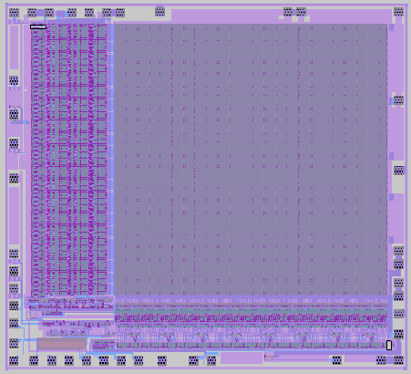
The objective of this project is to design a still-image sensor IC using standard digital CMOS technology. A prototype has been fabricated in a 1.2um CMOS technology through MOSIS. This circuit operates from a +5V supply and includes an electronic shutter.
The core of the image sensor is a 128x128 pixel array. Each pixel consists of four PMOS transistors and a photo-diode made up of a p-diffusion/n-well junction. The parasitic vertical PNP structure of the photo-diode provides anti-blooming suppression. An electronic shutter is implemented with a PMOS switch. Incident light on each pixel generates a photo-current that is integrated and stored as a voltage. A transconductance buffer in the pixel converts this voltage into a current that is read out on the column line. The use of a current readout signal minimizes the voltage swing required on the highly capacitive column lines. For each column a readout amplifier converts the current-mode signal from the selected pixel into an offset- compensated analog voltage sample that is multiplexed out sequentially. Digital shift registers are used to scan the columns and rows.
Faculty:
Bruce Wooley
Students: Chye-Huat Aw, Julie Segal
Physicists (Univ. of Hawaii): Sherwood Parker (Principal Investigator), Chris Kenney
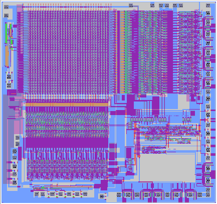
This project involves the design and fabrication of a pixel detector for high energy physics applications.
Pixel detectors provide the possibility of much higher signal-to-noise ratios than those of silicon strip detectors, where the ionization charge is collected on structures with typical capacitances of 5-20pF. In contrast, the elements of pixel detectors tend to be several orders of magnitude smaller and the input signal voltages are correspondingly greater, allowing the possibility of obtaining signal-to-noise ratios ten or more times larger than those typical of strip detectors. With the above characteristics, pixel detectors have several performance advantages over strip detectors in potential high energy particle vertexing systems. They provide unambiguous, two-dimensional position information. Their small dimension also allows much finer spatial resolution. With high signal-to-noise the active thickness of the substrate can be reduced, thus making the detector useful for particles with momenta less than several GeV/c which are susceptible to multiple scattering.
Our detector combines a PIN-diode based detecting element with readout circuitry in a single piece of 300um thick, high-resistivity, P-substrate silicon. During operation the very lightly doped substrate is fully depleted. When a high energy particle traverses through the substrate, it generates electron-hole pairs. Holes, guided by the electric field lines, get collected by the p-type collection electrode at the top of the array. This charge is integrated and stored as a voltage signal on the gate of a MOS transistor. These voltages resulting from hits by high energy particles will be readout upon receipt of a trigger signal from the system.
A prototype has been designed and fabricated for a fix target high energy physics experiment. The core of the detector is a two-dimensional array of detecting pixels. At the periphery are row and column sense amplifiers for sparse readout capability. Upon receipt of the trigger signal from the sytem, the row and column sense amplifier's hit registers will be scanned to determine the location of hits. The output consists of analog pulse height (which is a measure of the amount of ionization charge collected) and the xy coordinates.

![]()
 Integrated Circuits Lab