
Reduction of power dissipation by approximate processing is possible because of the nature of audio signals. In conventional filters, the order is fixed based on worst-case signal statistics, inefficient if the worst case seldom occurs. More flexibility is incorporated using adaptive filtering algorithms, characterized by ability to dynamically adjust processing to the data using feedback. Approximate processing involves dynamic adjustment of the filter order and leads to filtering solutions in which the stop- band energy in the filter output is kept below a specified threshold while using as low a filter order as possible. Power is reduced by dynamically minimizing digital filter order.
To reduce power and area overhead, the filter order is restricted to vary among four different values: Order0 < Order1 < Order2 < Order3. The full order of the filter corresponds to Order3, and the minimum order, that is 3 in this design, corresponds to Order0. The four order sizes are divided by three threshold values, T1 < T2 < T3. When the computed stop-band energy is between Ti and Ti+1, the filter order is equal to Orderi. Each threshold value Ti is determined by the specified output stop-band energy and the stop-band energy in the frequency response of filter order Orderi. Larger Ti corresponds to a larger filter order Orderi given a fixed output stop-band energy.
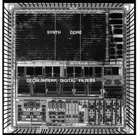
The decimation filter for the oversampled A/D converter is a 3-stage linear-phase decimation filter. The first-stage sinc filter does not use adaptive approximate filtering. Only the first half-band filter(order 19) and the second half-band filter (with order 61) are dynamically adjusted. Similarly, the interpolation filter for the oversampled D/A converter is a four-stage linear-phase interpolation filter. Only the three half-band filters of orders 61,19 and 11 emply dynamic filter order.
The two half-band filters in A/D converter and the three half-band filters in D/A converter are implemented by a programmable processor. The processor employs memory addressing for multi-rate digital filters. Processor components include data RAM, coefficient/control ROM and 22b arithmetic unit(AU). The AU performs basic arithmetic opersations: addition of pairs of delayed filter inputs stored in the data RAM, multiplication by coefficients stored in the ROM and accumulation of products to form the filter output. Computation of the feedback quantity for filter update is also implemented by this unit. The coefficient/control ROM contains control instructions for the processor. The 256 locations in the ROM are accessed sequentially via an 8b counter driven by the 12.3 MHz filter clock.
The powering-down control of the approximate filtering is implemented by maintaining a 2b level register and the 2b grade field associated with each instruction. A powering-down control block is inserted between the ROM and the AU to control instruction issue. When the level value is less than the grade value of an instruction, the stop-band energy is so weak that the instruction can be powered down by generating a virtually powerless NOP for the AU; otherwise, if the levle value is greater than or equal to the grade value, the stop-band energy is strong enough to turn the instruction on and the instruction is issued. The partitioning of the full filter in terms of instructions is programmed by assigning each instruction an appropriate 2b grade value. Once the partitioning of the full filter order is determined, the output stop-band energy is controlled by assigning each threshold Ti an appropriate value.
The stop-band energy statistics influence the power performance of approximate filtering. In decimation and interpolation, the stop-band energy increases with input signal strength. When a signal with strong stop-band energy arrives, a larger fraction of the time, the level values are high enough to turn on the instructions and consume more power. If the input signal and stop-band energy are weak, the instructions are turned on for shorter time and power performance increases.
When the input signal is at full scale, simulated and measured power reduction ratios are 42% and 36% for decimation and 21% and 17% for interpolation. Measured power performance is a bit lower than simulation results due to idle power dissipation of the NOP instruction, assumed zero-power in simulations. Idle power dissipation comes from the coefficient/control ROM, that runs even though the instruction is masked. When the input signal is attenuated, the percentage of power-down instructions increases and the power performance improves. When the input signal is attenuated by > 40dB, the power reduction ratio saturates at about 57% for decimation and 40% for interpolation. Power dissipation of the full-order filter is 13.6mW for decimation and 14.8mW for interpolation operating from a 5V supply at 12.3MHz clock. One pair of decimation filters and two pairs of interpolation filters occupy 8.02 mm2 in 0.5um CMOS.

![]()
 Integrated Circuits Lab