
With the advent of high-performance Digital Signal Processing (DSP) systems there is an increasing demand for high-resolution, high speed Analog to Digital Converters (ADCs). These ADCs are used in many applications such as medical instrumentation, imaging systems, and communcations. For example, the rapidly growing field of cellular and personal communications requires ADCs for tasks ranging from basic baseband signal conversion to eliminating the need for heterodyne processing through sub-sampling . The use of ADCs in these systems alleviates the need for expensive and complicated signal processing and and allows more robust, and typically less expensive, DSP algorithms to be utilized.
For cellular applications, an ADC's typical required performance is a spurious free dynamic range, SFDR, of at least 65dB and a sampling rate of at least 10MHz. Until now, high performance ADCs meeting these specifications have been implemented almost exclusively with expensive hybrid techniques. The primary reason for this is the difficulty in achieving highly linear components monolithically. High-speed ADCs are capable of achieving only 8-10bits of linearity in most IC processes without the use of component trimming or calibration techniques. Trimming, like the hybrid technique (which incorporates trimming), is undesirable due to its expense. Furthermore, because this technique is typically performed only once at the factory, its effectiveness is limited due to component aging and deviations in the ADC's operating conditions from those under which trimming was performed.
Calibration, on the other hand, is a potentially low-cost solution that can provide an ADC with the required performance in the presence of component aging and environmental fluctuations. In general, calibration attempts to linearize an ADC's transfer characteristic by measuring multiple points along the ADC's transfer curve and applying a sufficiently linearizing algorithm. A great deal of effort has been exerted recently in developing calibration techniques that enable present day processing technology to inexpensively produce high-speed, high-linearity ADCs.
The major disadvantage of most of these calibration schemes is that the ADC's operation must be interrupted to perform re-calibration. This type of calibration is, therefore, inappropriate for applications that require long-term, continuous operation of the ADC. For instance, in communications and telemetry gathering systems, the need for backup ADC's and/or the need to go off line for re-calibration increases cost and complexity. In a variety of applications where these systems are required, the environment can change so rapidly (consider a satellite, for example) that gaps in the gathering or transmitting of information can occur because the electronic systems cannot compensate quickly enough. In these applications, system redundancy and climate-control are essential and, therefore, costs are driven up. In general, any application that subjects ADC's to either long periods of operation and/or rapidly changing operating conditions are those in which most presently available calibration techniques would not perform adequately.
Continuous calibration is one possible method that can satisfy the stringent demands of applications like the ones described above. Previously presented continuous calibration schemes are limited in that they either require extra clock cycles therby decreasing speed or that they require an extra high-linearit ADC. The need for a high-linearity ADC that necessarilly operates at a lower speed then the ADC being calibrated results in frequency dependent errors not being removed, increased complexity, and increased power dissipation.
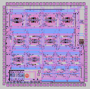
In this research we have explored the use of continuous calibration in the design of ADCs for applications such as cellular or personal communication systems. ADC's used in these systems must operate at relatively high speed (>10MHz) and have high linearity (>65dB SFDR). If portablility is is desired, then all of these specifications must be met with low power.
Our calibration architecture incorporates an extra stage that is calibrated outside of the pipeline and is subsituted in for a pipeline stage that requires re-calibration. As long as the stage being removed has finished its conversion phase and hasn't begun to sample a new input, the pipeline's operation will remain unaffected. This cycle can be repeated periodically in order to guarantee that the converter is always calibrated.
Our calibration technique dynamically adjusts the transfer functions of the error causing stages so that the major types of errors are removed. The corrected transfer characteristic of the ADC has high linearity with an input referred offset error and a gain error. These errors are easily removed digitally with a simple subtraction and multiplication. The major advantages of our calibration scheme compared with previously presented continuous calibration schemes are that the conversion speed of the ADC is essentially unaffected and that no extra high-linearity data converter is required.

![]()
 Integrated Circuits Lab