Faculty:
Bruce Wooley
Student: Sha Rabii
![]()
This research deals with the impact of various circuit and architectural configurations on the power consumption of sigma-delta analog-to-digital converters. The focus is data conversion with 13 to 16 bits of resolution and 20 to 200 kHz of signal bandwidth in a low voltage (<2V) environment. Several circuit topologies have been evaluated including switched-current, continuous-time, and switched capacitor. The switched-capacitor method was used throughout this work for its linearity and, contrary to popular belief, its relatively low power dissipation at low supply voltages.
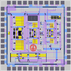
Two sigma-delta modulators have been fabricated to demonstrate the validity of the analytical results. The first achieved 92 dB of dynamic range over a 25 kHz bandwidth while dissipating 5.4 mW from a 1.8-V power supply and was fabricated in a 1.2-um CMOS technology without low threshold devices. The second chip achieved 99 dB of dynamic range over a 25 kHz bandwidth while dissipating 2.5 mW from a 1.8-V supply and was fabricated in a 0.8-um technology without low threshold devices. Both chips operate down to a 1.5-V supply voltage although at some cost in linearity.
![]()
![]()
![]()
From 1989 to 1992, he was a Manufacturing Development Engineer at Hewlett-Packard, Santa Rosa, CA, where he was responsible for SAW and optical devices. During the spring of 1994, he worked on a low-power A/D converter for hearing aids at Siemens, Munich, Germany. From January 1997 to March 1999, he was a Staff Design Engineer at Level One Communications, San Francisco, CA, where he designed circuits for CMOS wireless transceivers and a voiceband codec. From April 1999 to August 2001, he was at Atheros Communications, Sunnyvale, CA, as Analog Design Manager engaged in the design of CMOS transceivers and data conversion circuits for wireless LAN applications. In August 2001, he cofounded Aeluros Communications, Mountain View, CA, a provider of integrated circuits for 10Gb/s Ethernet. Dr. Rabii co-founded Arda Technologies in October 2006 and serves as the company's CEO. Arda Technologies is a provider of custom designed mixed-signal and analog integrated circuits.
Visit the Arda Technologies web site.
Email: sha@par.Stanford.EDU