
Transceivers for modern wireless and wireline communications systems typically include fast, low-power, low-voltage, A/D converters realized in deep-submicron CMOS. For example, the 1000BASE-T Ethernet protocol requires the use of converters with a bandwidth of 60MHz and a resolution of 7 to 9 bits. Similarly, receiver architectures for wireless standards such as the IEEE 802.11a/g also use such high-speed, medium-resolution ADCs. In both cases, low power consumption is a key performance metric. Previously reported stand-alone Nyquist ADCs operating at a rate of 150 MSamples/sec with a resolution of 8 bits typically dissipate more than 100mW of power.
This work introduces a low-power A/D converter suitable for high bandwidth communications applications [1]. The front-end track-and-hold circuit of the converter is followed by a 2.8-bit pipeline stage that comprises two time-interleaved residue generation paths. Two 1.5-bit pipeline stages, implemented using switched-capacitor circuits, follow for each of the residue paths. After digital error correction, each path alternately contributes the 4 most significant bits of the conversion. Each of the two interleaved residue paths concludes with a "backend" A/D converter that encodes the 4 least significant bits and employs a simple folding technique to reduce the number of comparators required.
Highlights of the complete ADC include the design of the front-end track-and-hold circuit and signal scaling that is used to reduce the full scale range of the residue of the first pipeline stage. The signal scaling facilitates the design of a high-speed, high gain operational amplifier with very low power dissipation.
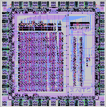
An experimental prototype has been integrated in a 0.18um CMOS technology and operates from a 1.8-V supply. At a sampling rate of 150MSamples/sec, it achieves a peak SNDR of 45.4dB for an input frequency of 80MHz. The power dissipation is 71mW.
![]()
![]()
 Integrated Circuits Lab
 Stanford University
 National Technical University of
Athens
National Technical University of
Athens