Faculty:
Bruce Wooley
Student: Tallis Blalack

Research efforts at Stanford have delved into the design and integration of high-performance mixed-signal circuits. In the case of oversampled sigma-delta converters, architectural enhancements have resulted in designs limited by circuit, rather than quantization, noise. In the course of this research it became obvious a better understanding of second-order noise mechanisms was essential to obtaining further improvements in performance. Therefore, we began to study the substrate coupling of digital switching transients into sensitive analog circuits by means of both experimental test structures and device and circuit simulations. Research in the initial phase of this effort focused on substrate noise in CMOS technologies wherein a lightly doped epitaxial layer is grown on a heavily doped bulk substrate. Both experimental observations and simulations indicate that transient induced noise spreads rapidly throughout an entire chip, and physical separation by more than four times the equivalent thickness of the epitaxial layer is of little use in isolating analog and digital circuits. In addition, it is clear that package inductance in series with the substrate contact will limit the extent to which substrate noise can be minimized. Although these initial experiments provide a much clearer picture of substrate noise coupling and the mechanisms involved, the experimental test structures are far simpler than the analog circuits used in high resolution data conversion interfaces.
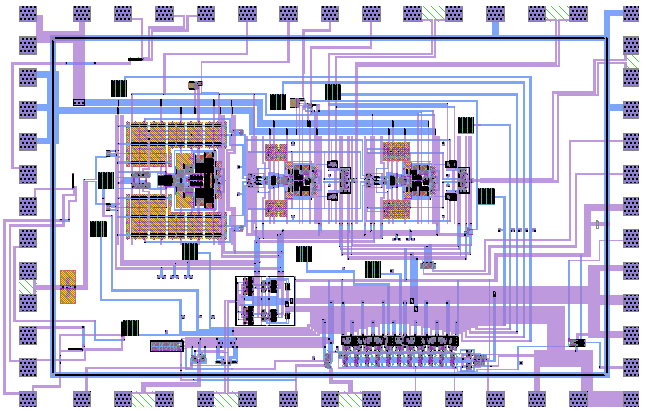
In order to move to a more representative test situation, a suitable test vehicle was chosen. A third order sigma-delta modulator, a 2-1 cascade designed in previous research with a dynamic range of over 100 dB, provided the needed properties of noise sensitivity, circuit complexity, and experimental flexibility. A control line was added to the modulator to turn off the second stage, changing the modulator from third order to second order, allowing experiments to be run on two different architectures. As different measurements are taken, the modulator output shows how an individual test affects the overall performance.
To perform these measurements, additional circuitry was added around the modulator to enable the injection of noise into the substrate. The substrate voltage excitations will affect transistor current flow in the modulator via threshold voltage variations (body effect) and capacitive coupling between the substrate and the gate, drain, and source nodes. To emulate digital switching noise, eleven 5-pF capacitors surround the modulator and are driven by large CMOS inverters. An on-chip shift register performs a serial to parallel conversion which enables independent control over each capacitor. In this manner locational sensitivities can be viewed and the amount of switching capacitance can be varied from 0 to 55-pF. Separate clock signals are available for the noise sources and the modulator allowing selection between on-chip and off-chip sources for the noise clock and a choice of a large swing or small swing clock for the modulator.
Some of the results of this work were presented at ISSCC in February of 1995. A significant performance reduction in the sigma-delta analog-to-digital converter was shown by introducing switching noise. Switching occurring before or at the sampling edge caused the most severe degradation, with as little as 20 pF of switching capacitance resulting in a 30 dB reduction in the signal-to- noise+distortion ratio for an input 5 dB below overload. When the switching noise was synchronized with the sampling clock, the substrate noise induced harmonic tones in the output, implying a signal dependent disturbance. The noise shaping attenuation of the sigma-delta converter leads us to the belief that the circuit is primarily sensitive to noise coupling in at the front end of the modulator. Current work is focused on simulating the experimental results obtained and investigation into lightly-doped bulk substates.

![]()
 Integrated Circuits Lab