
If the predictions of the great Nostradamus are correct, in about 1021 years after the massacre of huns by the Tatars, (about 10 years from now), analog to digital and digital to analog converter designers will be the rulers of the world of IC design. No matter how fast and accurate the digital portion of the chip is, the digital designers should wait in agony and fear to see how fast the interface is (which is always slower and less accurate than the DSP portion). But who dictates the overall speed/performance/accuracy? The mighty interface designer.
By now, you should all have guessed what topic I picked for my research: high velocity (oops, I meant speed), high resolution digital to analog (D/A) converters. And while I was waiting for my chip to be fabricated (which took more than twice the usual) I started reading the great Machiavellian books, to get ready to rule the world. Now, my chip is back and tested, and victory shall be mine!
We chose a multi-bit digital modulator, and used Philips' current calibration technique to overcome the nonlinearity inherent in multi-bit designs. The current calibration is an elegant, classic approach, and I highly recommend you to read the Philips paper to boost up your spirit on your bad hair days.
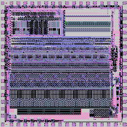
Finally, I made my chip, and it took forever to come back (literally). I will keep you all posted on the outcome! You are all more than welcome to light candles and pray for my dear chips to outperform my wildest dreams. I really appreciate your time and consideration.
Link to the group resource
page

CONTACT
Center for Integrated Systems, #067
Stanford University
Stanford, CA 94305
voice: (650) 725-4543
fax: (650) 725-3383
 Email:
katayoun@par.Stanford.EDU
Email:
katayoun@par.Stanford.EDU

 Integrated Circuits Lab